

PHYSICAL DESIGN COURSE
About us
Technoready is a reputed business organisation for professional trainings, manpower consultancy and electronics product development & s an established brand name for sourcing skilled electronics engineers to meet the rising demand of Electronics Systems Design in India.
Our mission
Etiam fringilla lobortis risus, sed accumsan enim rutrum vel. Aenean iaculis magna libero, at blandit augue rhoncus sed.
Pre-requisites
- Knowledge of Basics of Electronics, DigitalElectronics
DESCRIPTION
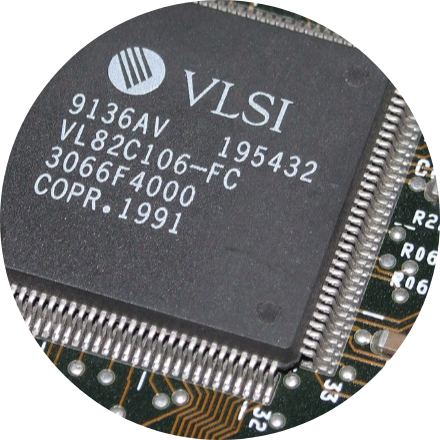
This is a basic program on VLSI(Very Large Scale Integration). Students will get good exposure of complete IC design flow. We will train students for developing digital logic design with hardware descriptive language Verilog HDL
FEATURES
- Knowledge of VLSI Design Flow
- Knowledge of Verilog HDL- RTL Coding & Synthesis
- Knowledgeof Logical Verification and Designing.
- Knowledge of FPGA
- Personal Experience of working with Live
Curriculum
| Section 1 | Introduction to VLSI Design |
| Section 2 | Overview of Digital Electronics |
| a. | Number Systems |
| b. | Converters |
| c. | Boolean Algebras |
| d. | Logic Gate |
| e. | K-Map |
| Section 3 | Combinational Logic Design |
| a. | Adder, Subtractor |
| b. | Comparators |
| c. | Multiplexer, Demultiplexer |
| d. | Encoder,decoder |
| Section 4 | Sequential Logic Design |
| a. | Latches |
| b. | Flip-Flops |
| c. | Counters |
| d. | Registers |
| Section 5 | Verilog HDLs Overview |
| a. | Design Hierarchy |
| b. | About HDL |
| c. | Advantage of HDL |
| d. | About Verilog |
| e. | Popularity of Verilog |
| Section 6 | Verilog Concepts |
| a. | Lexical conversion |
| b. | Datatypes |
| c. | System task & compiler |
| d. | Definition of Module |
| e. | Declaration of Ports |
| Section 7 | Gate Level Modelling |
| a. | About gate type modeling |
| b. | Delay concepts |
| c. | Examples |
| Section 8 | Date Flow Modeling |
| a. | About dataflow modeling |
| b. | Assignment |
| c. | Delay Control |
| d. | Operators |
| e. | Examples |
| Section 9 | Behavioral Modelling |
| a. | About behavioral modeling |
| b. | Structured procedures |
| c. | Initial and always |
| d. | Blocking and non-blocking statements |
| e. | Delay Control |
| f. | Conditional Statement |
| g. | Loops |
| Section 10 | Tasks and Function |
| a. | Difference between tasks and functions |
| b. | Declaration of functions |
| c. | Declaration of tasks |
| Section 11 | Modelling Technique |
| a. | Assign and deassign |
| b. | Force and release |
| Section 12 | User Defined Primitives |
| a. | About UDP |
| b. | Rules for UDP |
| c. | UDP installation |
| Section 13 | Apply Stimulus |
| a. | Need of TB |
| b. | About TB |
| c. | Type of TB |
| d. | Apply stimulus |
| Section 14 | Finite State Machine |
| a. | Definition of FSM |
| b. | About State machine |
| c. | Step to design |
| Section 15 | About FPGA |
| a. | Introduction to FPGA |
| b. | FPGA architecture |
| c. | Logic Element |
| d. | Programmable wiring |
| e. | Technology |
| f. | SRAM based FPGA |
| g. | Configuration vs Programming |
| Section 16 | About FPGA |
| a. | About synthesis |
| b. | Simulationvs Synthesis |
| c. | How is synthesis used |
| d. | Impact of logic synthesis |
| e. | Synthesis process |
| Section 17 | Verification Technique |
| a. | Formal verification |
| b. | Circuit verification |
| Section 18 | Project work Preparation |
| a. | Selection of project |
| b. | Software design of project |
| c. | Test method(hardware and software) |
| Section 19 | Documentation |
| a. | Preparation of synopsis |
| b. | Preparation of PPT |
| c. | Preparation of project report |
| d. | Preparation of code documentation |
| e. | Submission of documents |
